Published By: Silicon India
Date: 9th September 2024
Media Type: Digital

- | Published On:
DALL-E Prototyping Is Not A Production Scaling a semiconductor design from prototype to production is where promising ideas meet harsh reality. A prototype demonstrates feasibility and shows that a concept can work under controlled conditions but is not a finished product. Many teams celebrate the first silicon success, only to realize later that this milestone marks the beginning of the journey to market, not the end. The challenges of scaling are often underestimated. At advanced nodes, a single complete mask set can cost upward of a million dollars. A seemingly minor design change, such as adjusting a clock buffer or modifying a pin assignment, can require a complete mask revision and push schedules back by several weeks. On the other hand, custom test boards, essential for silicon […]


The Real Cost Of Scaling A Semiconductor Design From Prototype To Production
 ByChetan Arvind PatilPublished On: May 24, 2025
The Semiconductor Product Is More Than Just Silicon
ByChetan Arvind PatilPublished On: May 17, 2025
The U.S. Semiconductor Supply Chain – Now And The Future
ByChetan Arvind PatilPublished On: May 10, 2025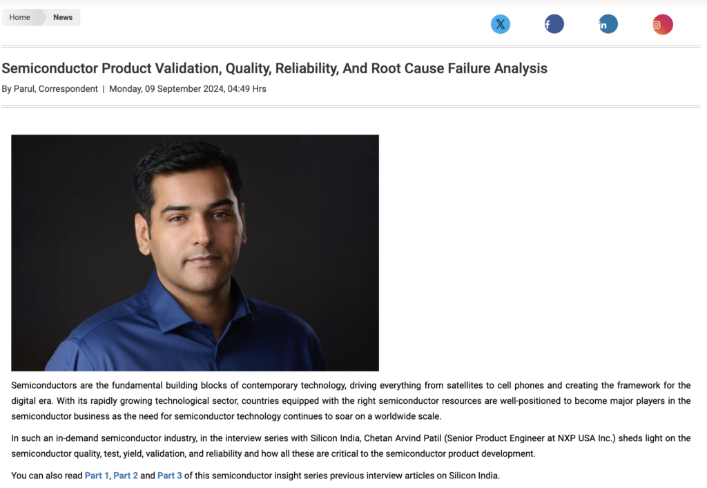
Semiconductor Product Validation, Quality, Reliability, And Root Cause Failure Analysis
Test And Yield Challenges of Chiplet-Based Semiconductor Products
Published By: Chiplet-Marketplace
Date: 23rd December 2024
Media Type: Digital

Cost Challenges Of Getting Advanced Semiconductor Products To Market
Published By: Electronics Product Design And Test
Date: May 2025
Media Type: Online Media Website And Digital Magazine
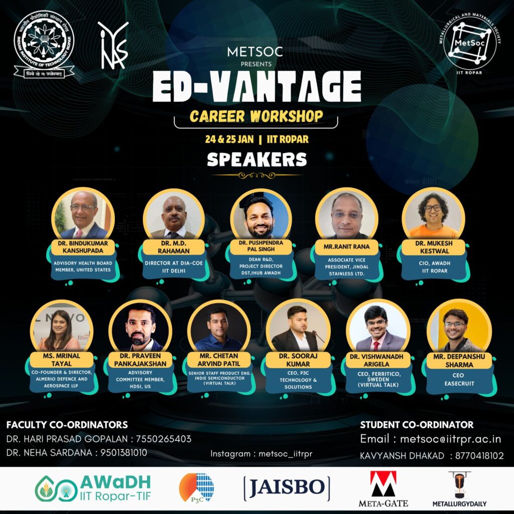
Semiconductor Career Opportunities In Metrology And Materials Science
- Hosted By: Indian Institute of Technology, Ropar
- Location: Rupnagar, Punjab, India (Virtual)
- Date: 23rd/24th January 2025
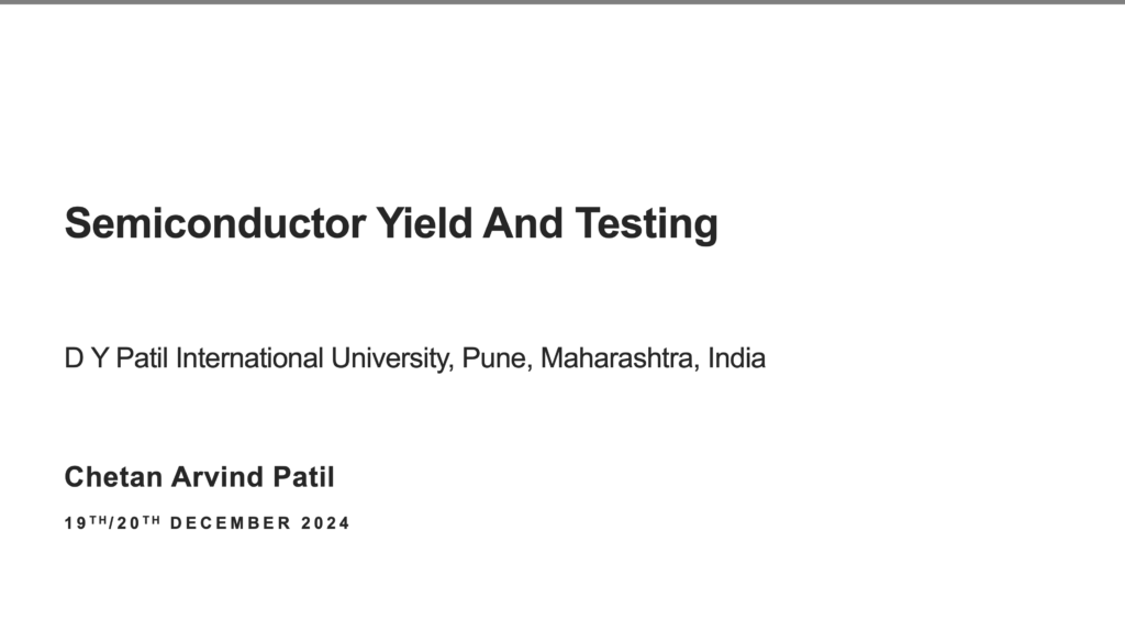
Semiconductor Yield And Testing
- Hosted By: D Y Patil International University
- Location: Pune, Maharashtra, India (Virtual)
- Date: 19th/20th December 2024
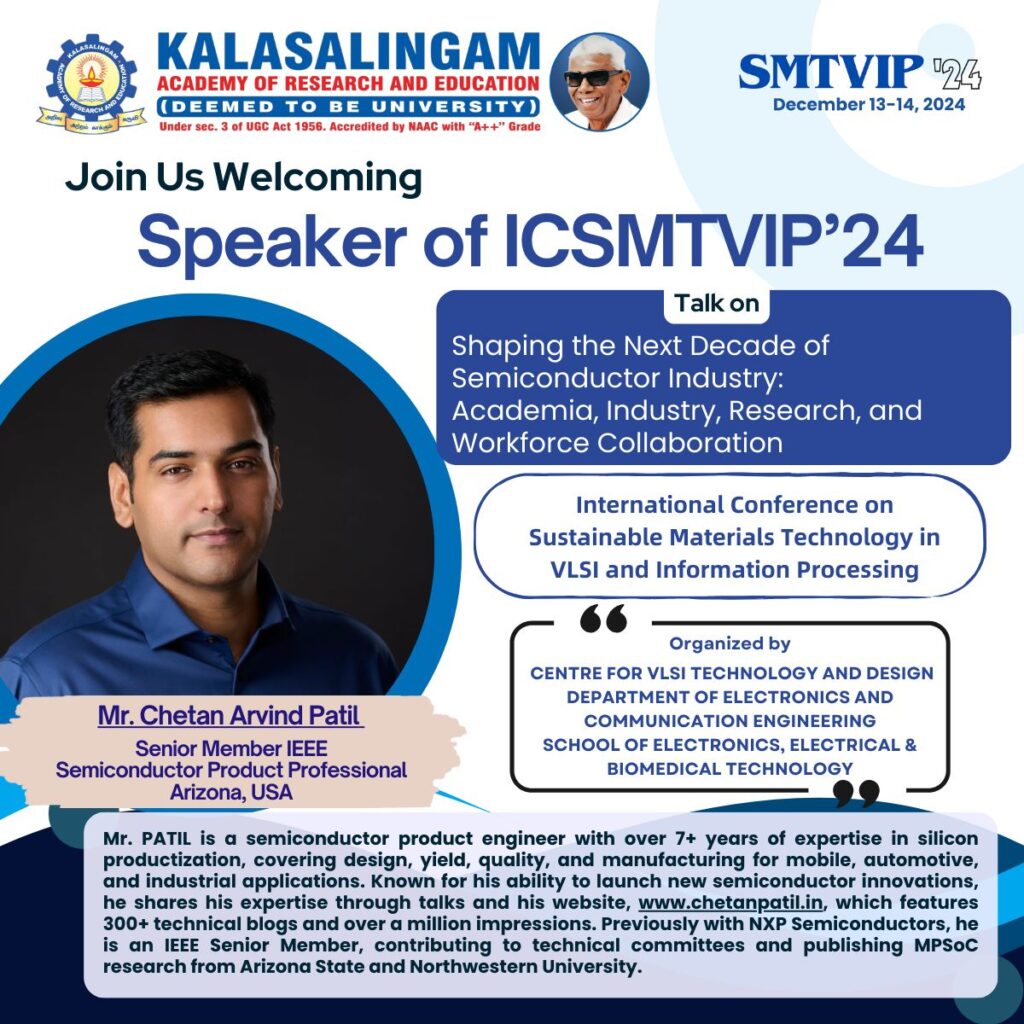
Shaping The Next Decade of The Semiconductor Industry: Academia, Industry, Research, and Workforce Collaboration
- Hosted By: Kalasalingam University
- Location: Srivilliputtur, Tamil Nadu, India (Virtual)
- Date: 13th/14th December 2024
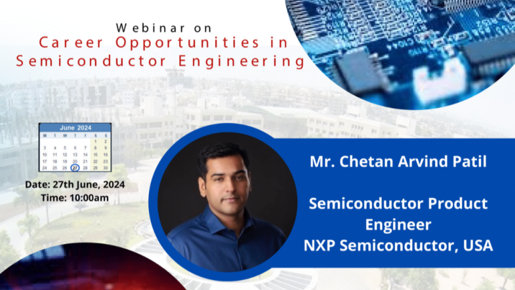
Career Opportunities In Semiconductor Engineering
- Hosted By: D. Y. Patil International University
- Location: Pune, Maharashtra, India (Virtual)
- Date: 26th/27th June 2024


Discover The World Of Semiconductor
Explore my website and learn about semiconductor including information about all of my talks, research, media articles and mentions
Let us also connect to explore ideas, discussing speaking opportunities, authoring a media article or even an interview including the endless possibilities that the semiconductor industry has to offer.