Image Generated Using DALL-E
Why New Materials Are Needed
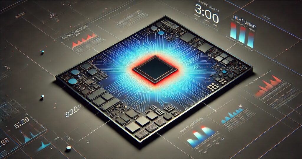
The semiconductor industry has been built on the backbone of silicon for decades. While silicon has served us well, its physical limitations are becoming more apparent as we push the boundaries of device miniaturization and performance. The demand for higher speed, better energy efficiency, and more robust thermal management in applications ranging from smartphones to electric vehicles has exposed silicon’s constraints. These challenges of searching for new materials are not just an option but a necessity to sustain the pace of technological innovation.
Major reasons, new materials are needed:
- Performance Constraints: Silicon struggles to handle high power and frequencies efficiently, leading to energy losses and heat generation. This limits the performance of power electronics, RF devices, and other high-frequency applications.
- Thermal Management Issues: With the miniaturization of components, managing heat within semiconductor devices is becoming increasingly challenging. Silicon’s thermal conductivity is inadequate for many high-power applications, leading to overheating and potential device failure.
- Energy Efficiency: As global energy demands rise, improving energy efficiency in all electronic devices is crucial. Silicon’s limitations in this area hinder advancements in areas like electric vehicles, renewable energy systems, and portable electronics.
- Emerging Technologies: Future technologies like quantum computing, AI, and advanced telecommunications require materials with properties that silicon cannot provide. For instance, two-dimensional materials and wide-band gap semiconductors can operate under conditions that silicon cannot withstand, offering the potential for new device architectures and applications.
- Sustainability and Supply Chain: The production of silicon-based semiconductors is resource-intensive and contributes to environmental challenges. Additionally, geopolitical issues around silicon supply chains highlight the need for alternative materials that are more sustainable and accessible.
Examples Of Promising New Materials
As the demand for advanced electronic devices continues to grow, the semiconductor industry must look beyond traditional silicon to meet emerging technologies’ performance, efficiency, and scalability needs. This shift has led to exploring several promising new materials that offer unique properties and advantages. Below is a comparison of these materials and their potential impact on semiconductor innovation.
| Material | Key Properties | Applications | Advantages |
|---|---|---|---|
| Gallium Nitride (GaN) | High electron mobility, high breakdown voltage | Power electronics, RF devices | Smaller, more efficient power converters; high-frequency performance |
| Silicon Carbide (SiC) | High thermal stability, high voltage capacity | Electric vehicles, power grids | Reduces energy losses, operates under high temperatures and voltages |
| Cubic Boron Arsenide (c-BAs) | Exceptional thermal conductivity | High-power electronics | Efficient heat dissipation, improves device reliability |
| 2D Materials (Graphene, MoS₂) | High carrier mobility, flexibility | Flexible electronics, sensors, transistors | Ultra-thin, flexible devices, high-speed transistors |
| Indium Gallium Arsenide (InGaAs) | High electron mobility, direct bandgap | High-speed transistors, optoelectronics | Ideal for high-frequency communication, lasers, and photodetectors |
The integration of these new materials into semiconductor manufacturing is crucial for breaking through the limitations of silicon. Each material offers distinct advantages that could drive innovation across various applications, from power electronics to flexible devices. With ongoing research and development, these materials will play a pivotal role in shaping the future of the semiconductor industry, enabling the development of faster, more efficient, and more versatile technologies.

Role Of AI And Advanced Computation In Material Discovery
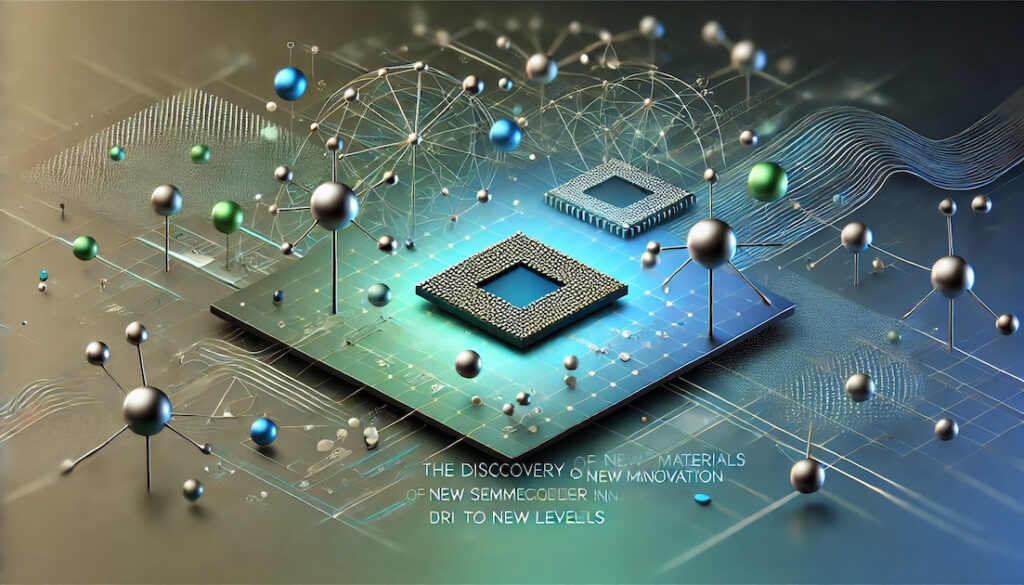
The discovery of new materials has traditionally been a slow and expensive process, relying heavily on trial and error in laboratories. However, the integration of AI and advanced computational methods is not just changing, but transforming this landscape. AI can predict material properties, simulate interactions, and identify promising candidates much faster than traditional methods, inspiring a new era of material discovery.
AI-driven material discovery significantly accelerates the process by analyzing vast datasets to predict material behavior, reducing the time required for initial screenings. Machine learning models optimize fabrication processes by simulating various manufacturing conditions and pinpointing the best methods to achieve high-quality materials. Computational tools enable high-throughput screening, rapidly identifying promising material combinations that would take years to discover through conventional methods. By integrating experimental data with theoretical models, AI platforms provide a comprehensive understanding of material properties, allowing for rapid design iterations and the discovery of tailored materials for specific applications.
IBM’s Deep Search Platform: IBM uses AI-driven platforms like Deep Search to analyze massive datasets of material properties and accelerate the identification of promising candidates for semiconductor applications. The platform can predict material behavior under various conditions, aiding in faster discovery and optimization.
Meta’s Open Catalyst Project: This project leverages machine learning to discover new catalyst materials for sustainable energy production. By training models on large datasets, they can predict the reactivity of new compounds more efficiently, which also lies in semiconductor material discovery as well.
Google’s Materials Discovery AI: Google’s AI research focuses on predicting properties of inorganic materials using neural networks. This model helps screen potential materials for electronics, predicting properties such as bandgap and stability.
By harnessing the power of AI and computational models, researchers can explore a broader range of materials, significantly accelerating the transition from theoretical concepts to practical applications. This approach not only speeds up the discovery process but also plays a crucial role in reducing costs and environmental impact. The promise of a more sustainable and scalable future for material innovation in the semiconductor industry is within reach, thanks to AI-driven material discovery.
Challenges In Integrating New Materials
While GaN and SiC have established fabs, integrating them into the broader semiconductor manufacturing ecosystem still presents challenges. The main issues include specialized equipment, as these materials require different processing conditions than silicon. Quality control, yield optimization, and maintaining high-performance consistency at scale are still complex tasks. Despite these challenges, existing fabs demonstrate the growing feasibility and adoption of GaN and SiC, but further innovation in manufacturing processes is necessary for widespread integration and efficiency improvements.
On top, integrating new materials like Cubic Boron Arsenide (c-BAs), 2D materials (Graphene, MoS₂), and Indium Gallium Arsenide (InGaAs) into semiconductor manufacturing faces several challenges. For c-BAs, large-scale production remains difficult due to the complexity of growing high-quality crystals. 2D materials face fabrication issues, particularly in maintaining stability and avoiding defects during integration with existing processes. While promising for high-speed applications, InGaAs suffer from lattice mismatch with silicon, which can lead to defects and reliability concerns and require advanced techniques for seamless device integration.
Additionally, achieving high-quality interfaces between new materials and silicon is another hurdle, as poor interfaces can introduce electronic defects. Moreover, while promising in labs, scaling these materials for mass production while keeping costs in check remains a daunting task. Overcoming these challenges requires innovative fabrication techniques and industry collaboration. But above all, it demands significant investment in research and development. The urgency of this investment cannot be overstated.