Image Generated Using DALL-E
Semiconductor Defect Pattern Analysis
The relentless drive for higher performance, lower power consumption, and increased functionality in semiconductor devices has led to unprecedented complexity in semiconductor manufacturing processes. As technology nodes shrink below 3nm and the adoption of 3D structures, such as GAAFETs, becomes widespread, the variability introduced by intricate process steps, material interactions, and equipment behavior poses significant challenges. Traditional yield analysis methods, which primarily rely on statistical summaries and post-mortem evaluations, are no longer sufficient to address these complexities.
In this evolving landscape, defect pattern analysis has emerged as a methodology for identifying, understanding, and mitigating yield-limiting mechanisms at both macro and micro scales. Defect pattern analysis systematically identifies and characterizes recurring defect trends across wafers, lots, and production lines. Unlike random defects, which occur sporadically and are often isolated, systematic defects are reproducible and stem from persistent issues related to process integration, equipment-induced anomalies, design rule violations, or material inconsistencies.
These defects manifest in spatial patterns, such as edge-localized clusters, center-focused anomalies, or stepper field-dependent distributions, each offering critical insights into underlying process deficiencies. If not promptly detected and addressed, these defects can significantly degrade electrical performance, reliability metrics, and, ultimately, the economic viability of semiconductor products.
Understanding Defect Patterns
Defect patterns in semiconductor manufacturing are intricate signatures that reflect the underlying health of the fabrication process. Analyzing these patterns enables the identification of process anomalies and equipment-related issues that impact yield.
In semiconductor manufacturing, defects can be broadly categorized into different types based on their occurrence, origin, and distribution. Types of Defects include Random Defects and Systematic Defects. Random defects are sporadic issues that arise due to factors such as contamination, transient process conditions, or environmental disturbances. They are unpredictable and typically isolated. On the other hand, systematic defects are repeatable and consistent, often stemming from process design flaws, equipment malfunctions, or material inconsistencies, making them easier to detect and analyze over time.
The Sources of Defects are diverse and can occur at various stages of the fabrication process. Lithography Issues, for example, result from misalignment, exposure errors, or anomalies in the photoresist layer, leading to pattern deformation. Etching Variations arise due to over-etching, under-etching, or micro-masking effects, which can compromise feature integrity. Chemical Mechanical Planarization (CMP) Defects are related to issues like dishing, erosion, or irregularities caused by slurry particles, impacting the planarity of wafer surfaces. Additionally, Material Impurities, such as contaminants or non-uniform material deposition, can introduce microscopic defects that affect device performance and reliability.
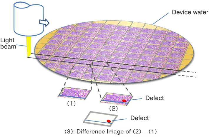
When it comes to the Classification of Defects, they are often grouped based on their spatial distribution and recurrence patterns. Clustered Defects are grouped in specific wafer regions, indicating localized process issues that may be tied to equipment or process variations. Repeating Patterns refer to defects that consistently occur in the exact locations across multiple wafers, signaling systematic problems often related to equipment faults or design-related challenges. Edge Exclusions are defects concentrated near wafer edges, typically resulting from process non-uniformities or handling errors during manufacturing. Lastly, Isolated Anomalies are defects that appear randomly across the wafer, usually caused by transient process disruptions or random contamination events.
Understanding these types, sources, and classifications of defects is critical for effective yield analysis. It enables semiconductor manufacturers to implement targeted corrective actions and improve overall process efficiency.

Technical Framework For Defect Pattern Analysis
The technical framework for defect pattern analysis in semiconductor manufacturing is a multi-layered approach designed to capture, process, and interpret defect data systematically. This framework integrates advanced inspection technologies, data acquisition methods, and sophisticated analytical algorithms to identify yield-limiting defects early in manufacturing.
At the core of this framework is the seamless integration of data from multiple sources. Ranging from in-line process control systems and metrology tools to electrical test results and environmental monitoring. By correlating defect data with process parameters and equipment performance metrics, manufacturers can uncover hidden relationships that might not be evident through traditional analysis methods. This comprehensive approach enhances the ability to detect subtle defect patterns, understand their root causes, and implement real-time corrective actions.
The following table outlines the key components of the technical framework and details the critical stages involved in defect data management and analysis.
| Data Collection And Acquisition | Mapping And Visualization | Pattern Recognition And Analysis | Process Optimization |
|---|---|---|---|
| Inspection Tools: Optical and e-beam systems for high-resolution wafer imaging to detect sub-micron defects. | Wafer Maps: Graphical displays showing defect locations to identify clusters, edge patterns, and systematic anomalies. | Statistical Analysis: Techniques like Pareto analysis and control charts to highlight defect trends and major contributors. | Real-Time Feedback Loops: Integration with MES (Manufacturing Execution Systems) for immediate corrective actions. |
| Process Data: Equipment logs, process metrics, and environmental data to correlate specific defects with process conditions. | Die Maps: Focused mapping of defect distributions within individual dies to identify layout-related and systematic issues. | Machine Learning Algorithms: Supervised and unsupervised models for defect clustering, anomaly detection, and predictive analytics. | Process Control Adjustments: Dynamic tuning of process parameters based on defect trends to minimize recurrence. |
| Test Data: Electrical test results from wafer probing and final test stages to link functional failures with physical defects. | Trend Charts: Time-based visualizations tracking defect density trends across production lots and process stages. | Root Cause Analysis (RCA): Combining defect data with process knowledge to trace anomalies to specific equipment or process deviations. | Preventive Maintenance Scheduling: Using defect trend data to predict equipment failures and proactively schedule maintenance. |
Importance Of Defect Pattern Analysis In Yield Enhancement
Defect pattern analysis is pivotal in semiconductor manufacturing, providing critical insights into yield-limiting factors. Its importance lies in detecting, classifying, and mitigating random and systematic defects that directly impact device performance, reliability, and production efficiency.
By identifying defect trends early in the process, manufacturers can implement targeted corrective actions, minimizing costly rework, material waste, and production delays.
Furthermore, integrating defect analysis with advanced data analytics and machine learning models enables predictive insights, allowing fans to proactively address potential yield excursions before they escalate into significant issues.
As semiconductor technologies advance to more complex nodes and architectures, defect pattern analysis becomes even more vital, serving as a strategic tool for continuous process improvement, cost reduction, and maintaining competitive advantage in a fast-evolving global market.