About

Hi, I am Chetan Arvind Patil (chay-tun – how to pronounce), a semiconductor professional whose job is turning data into products for the semiconductor industry that powers billions of devices around the world. And while I like what I do, I also enjoy biking, working on few ideas, apart from writing, and talking about interesting developments in hardware, software, semiconductor and technology.
I live in Aliso Viejo (CA, USA), a suburb of Los Angeles with a strong footprint in technology. Previously I have also lived in Glibert (AZ, USA), Chandler (AZ, USA), Tempe (AZ, USA), Evanston (IL, USA), Pune (MH, India), Mumbai (MH, India), Jalgaon (MH, India), Nagpur (MH, India) and Pathakhera (MP, India).
Nagpur, India.

I was born in India and grew up in Pathakhera and Nagpur. After high school, I earned a bachelor’s degree in engineering (B.E.) from the Pune Institute of Computer Technology, lovingly known by its acronym PICT, part of the University of Pune. I studied electronics and telecommunication engineering. My senior project was an Interactive TV System.
Pune, by the way, is the largest city in the state of Maharashtra and one of the largest in India. Some consider Pune the epicenter of the “New India” for its healthy mix of business and academia. Maharashtra is a fantastic place to visit. Lonely Planet has some nice things to say about my home state.


Pune, India.
None of my friends or family were surprised (pun intended) when I told them my next stop would be Arizona State University. I earned a second M.S. in Computer Engineering, focusing on Computer Systems this time. I studied power, performance, and energy management of heterogeneous architectures at ASU’s eLab, topics that are hot (no pun intended) just about everywhere. The work I carried out lead to papers getting published in journals and conference. I was mentored and advised by Prof. Umit Ogras.
ASU and Tempe remind me a lot of Pune – lots of high tech businesses working with higher education.

NXP Semiconductors, USA

After graduate studies, I worked at a company called NXP Semiconductors that designs and creates semiconductors for hundreds of industries with major focus on consumer and industrial market. Its headquarters are in The Netherlands with locations at tech hubs around the world.
I started there as an intern in the Chandler facility analyzing a large semiconductor data and was later hired as a Semiconductor NPI Product Engineer. I had the opportunity to work with very talented and interesting people, with few having more knowledge about cars than semiconductors (pun intended).


Indie Semiconductor, USA
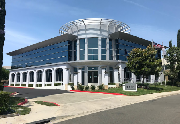
Right now, I am working at indie Semiconductor (Aliso Viejo in California), a pure-play automotive semiconductor company specializing in innovative and integrated solutions for automotive products.
My role as a Semiconductor Product Engineer involves leading and driving product development, ensuring design, yield, test and quality standards including optimizing processes to support the production of advanced semiconductor solutions tailored for the automotive industry.

Semiconductor And Beyond

Technology is a major part of today’s economy. That’s why I started writing my blog – to get more people talking about tech going on in the semiconductor and also in the wider world.
What kind of tech do you use, work on, dream about? Shoot me an email and maybe we can talk and share it with others!
