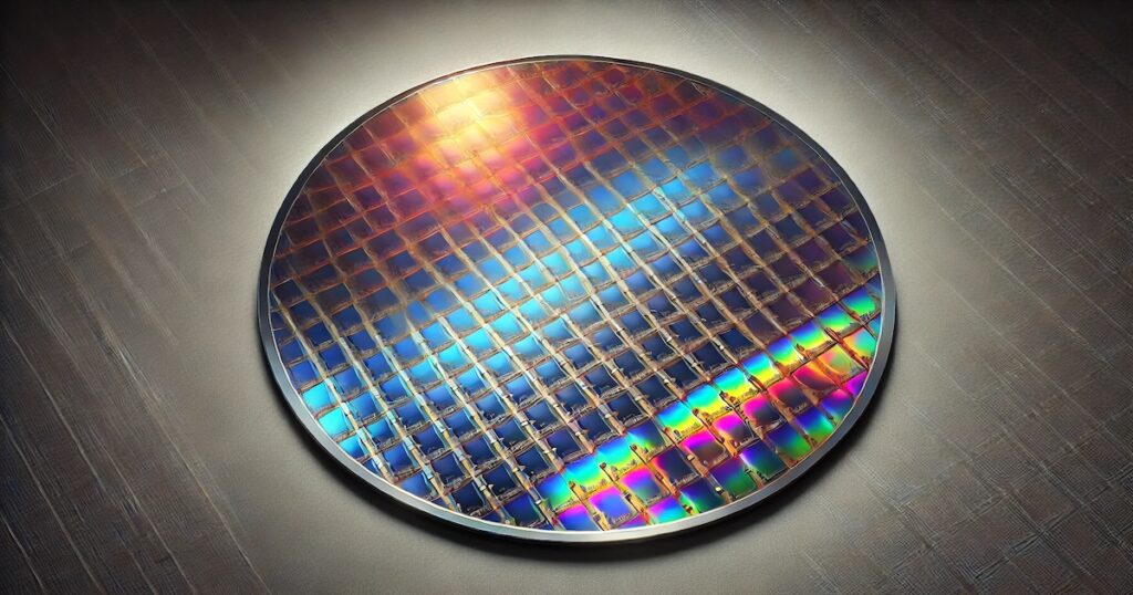
The Semiconductor Technical Approach To Defect Pattern Analysis For Yield Enhancement
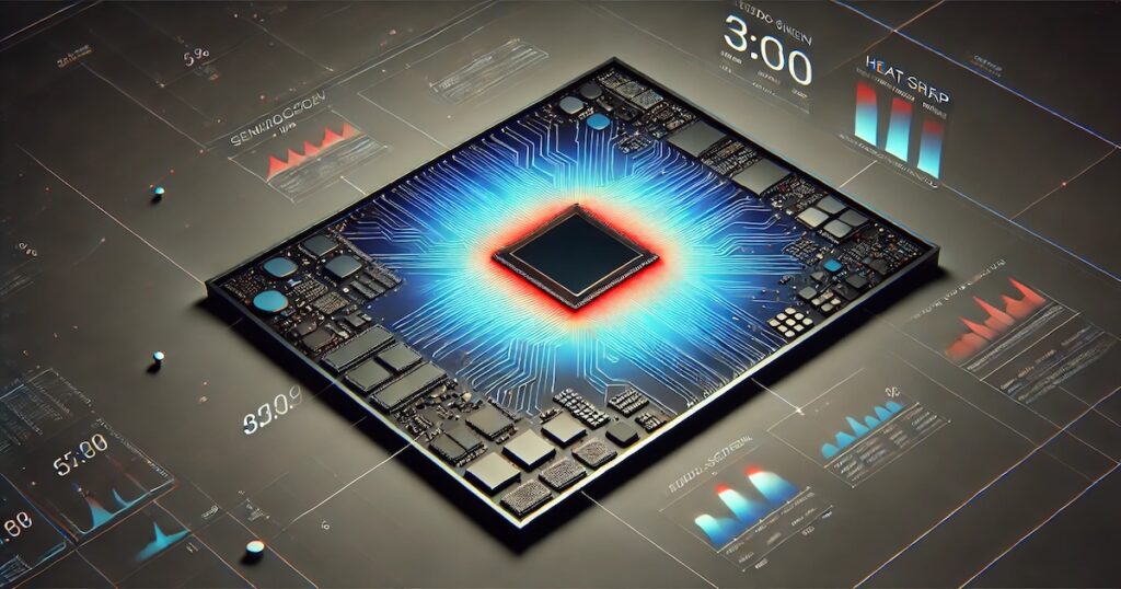
DALL-E Semiconductor Defect Pattern Analysis The relentless drive for higher performance, lower power consumption, and increased functionality in semiconductor devices has led to unprecedented complexity in semiconductor manufacturing processes. As technology nodes shrink below 3nm and the adoption of 3D structures, such as GAAFETs, becomes widespread, the