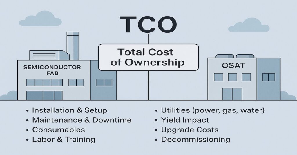
Image Generated Using DALL-E
Semiconductor Node Race
The semiconductor industry has long been dedicated to achieving exceptional performance, efficiency, and cost-effectiveness, primarily by advancing smaller process nodes. However, the increasing physical and economic challenges of further node shrinking have prompted a strategic shift in focus.
This exciting shift, known as ‘process flavor, ‘is not just a change in direction but a potential game-changer for the semiconductor industry. It involves the development of customized process technologies that are finely tuned for specific applications, marking a significant departure from the previous node-centric approach. With its potential to completely transform the industry, this innovative approach holds great promise for the future.
Process Flavor Vs Process Nodes
In the traditional semiconductor landscape, the drive towards smaller process nodes has been the hallmark of progress, symbolizing advancements in miniaturization, speed, and power efficiency. The smaller the node, the more transistors can be packed onto a chip, leading to higher performance and lower power consumption. This relentless pursuit, governed by Moore’s Law, has propelled the industry through remarkable technological milestones, with current leading-edge nodes reaching 3nm and 2nm. However, pursuing smaller nodes is becoming increasingly fraught with challenges, including astronomical RnD costs, manufacturing complexities, and diminishing returns in performance and efficiency gains.
Conversely, process flavor ushers in a new era in semiconductor manufacturing. Instead of fixating on the most minor possible node, process flavor advocates for customizing process technologies to meet specific application needs. This approach acknowledges that different applications, from high-performance computing to low-power devices, have unique requirements that can only be met through specialized process optimizations rather than a universal node shrinkage. By tailoring processes to specific use cases, manufacturers can achieve significant improvements in performance, cost efficiency, and energy consumption, all while mitigating the mounting challenges associated with node scaling. This strategy enhances technological versatility and market responsiveness and fosters innovation in areas where traditional node-focused approaches may need to be more effective.

Key Features Of Process Flavor And Nodes
As the semiconductor industry evolves, manufacturers’ strategies are diversifying to meet a variety of technological and market demands. Traditionally, the focus has been on shrinking process nodes to achieve higher performance and efficiency.
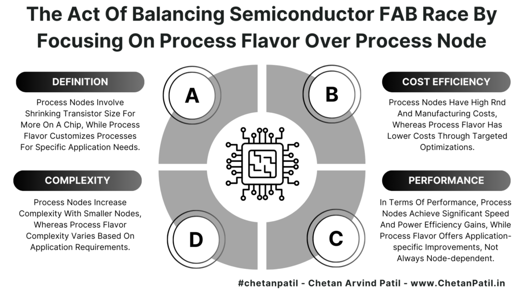
However, the emerging strategy of process flavor, which involves tailoring semiconductor manufacturing processes to specific application requirements, is gaining traction. This comparison table highlights the key differences between process flavor and process nodes, illustrating how each approach impacts various aspects of semiconductor technology and manufacturing.
| Feature | Process Flavor | Process Node |
|---|---|---|
| Definition | Customizing semiconductor processes for specific applications | Shrinking transistor size to achieve smaller nodes (e.g., 7nm, 5nm, 3nm) |
| Focus | Application-specific optimizations | Achieving the smallest possible transistor size |
| Cost Efficiency | Generally more cost-effective for targeted applications | Higher RnD and manufacturing costs due to complexity |
| Performance | Tailored performance for specific use cases (e.g., power efficiency, speed) | Higher performance potential through increased transistor density |
| Complexity | Increased design and manufacturing complexity due to customization | High complexity due to advanced lithography and fabrication techniques |
| Market Adaptability | Flexible and responsive to diverse market needs | Primarily driven by leading-edge markets and high-volume applications |
| Sustainability | Can optimize for energy efficiency and resource usage | High energy consumption and environmental impact at advanced nodes |
| RnD Investment | Focused on developing multiple specialized processes | Large investments required for each new node generation |
| Technological Challenges | Balancing customization with manufacturing feasibility | Physical and economic limits of silicon technology |
| Innovation | Encourages innovation in diverse application areas | Innovation primarily in lithography and transistor scaling |
Adopting a process flavor approach allows semiconductor manufacturers to tailor their technologies to meet the diverse demands of various applications, ranging from high-performance computing to energy-efficient devices. This strategy can lead to more sustainable practices and potentially lower development costs, as it avoids the escalating complexities associated with further node shrinking.
While process nodes have propelled significant technological progress, the transition to process flavor signifies a nuanced comprehension of market demands and technological capabilities. By harmonizing these two approaches, manufacturers can sustain innovation and deliver optimized solutions that precisely match the requirements of diverse applications, thereby fortifying the semiconductor industry’s resilience and adaptability.
Take Away
As the semiconductor industry navigates the challenges of advancing node shrinking, focusing on process flavor offers a balanced and strategic approach. By optimizing manufacturing processes for specific applications, semiconductor manufacturers can achieve significant performance and efficiency gains while managing costs and complexity. This shift addresses the limitations of pursuing ever-smaller nodes and paves the way for more sustainable and diversified technological advancements in the semiconductor industry.


