Image Generated Using DALL-E
Importance Of Semiconductor Yield
Semiconductor yield, the percentage of functional chips produced from a wafer, is a critical factor in the semiconductor industry. Yield influences production’s cost efficiency and determines manufacturing operations’ overall economic viability.
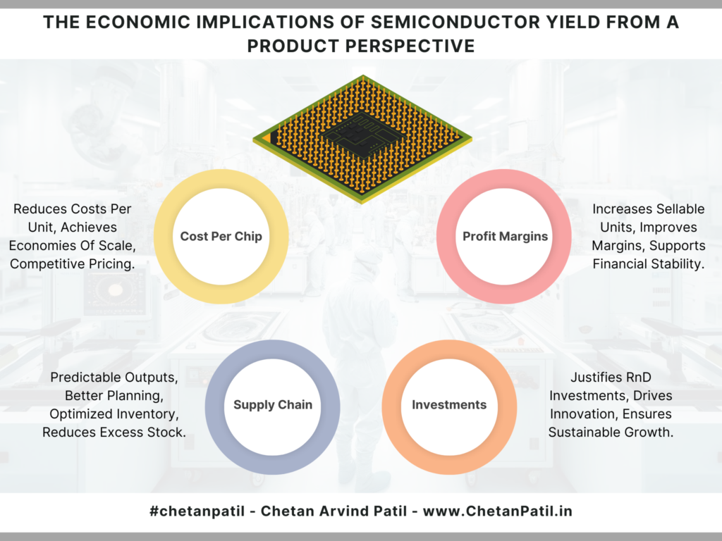
High yield directly impacts various economic aspects, including cost per chip, profit margins, market competitiveness, investment in technology, and supply chain efficiency.
Let us explore these implications from a product perspective, providing a comprehensive understanding of how yield affects the broader semiconductor landscape.
Key Metrics For Semiconductor Yield Analysis
As a first step, yield analysis involves understanding the percentage of functional chips produced from a wafer and identifying the factors influencing this outcome. By leveraging key metrics, manufacturers can gain insights into their production processes’ effectiveness, identify improvement areas, and make informed decisions to enhance yield performance.
This analysis improves the technical aspects of manufacturing and has profound financial implications, impacting profitability, cost management, and overall competitiveness. This section delves into the essential metrics used in semiconductor yield analysis, explaining their definitions, importance, and practical applications.
Die Yield: Die yield is the percentage of functional dies (chips) on a wafer. It measures the effectiveness of the manufacturing process. A high die yield indicates fewer defects and greater efficiency, leading to lower costs and higher profitability.
Defect Density (D0): Defect density is the number of defects per unit area on the wafer. Lower defect density indicates a cleaner manufacturing process and higher yield potential. It is an essential metric for assessing the quality of the production environment and processes.
Overall Yield: Overall yield considers multiple manufacturing stages and their yields. This metric provides a comprehensive view of the entire production process’s effectiveness. It highlights the importance of optimizing each stage to achieve a high yield, ensuring consistent and efficient production.
First-Pass Yield (FPY): Measures the percentage of products that pass all manufacturing stages without rework or repair. It is an indicator of process efficiency and quality. A high FPY reflects a well-optimized manufacturing process with minimal defects and interruptions, reducing production costs and faster time to market. Monitoring FPY helps identify areas in the production process that may need improvement to enhance overall yield and product quality.
Yield Model: Murphy’s model predicts yield based on defect density and die area. This model helps understand the relationship between defect density and yield, which helps make informed decisions about process improvements and defect reduction strategies.
Gross Die Per Wafer (GDW): Gross die per wafer is the total number of dies that can be produced from a single wafer. This metric helps estimate the potential production volume based on the wafer’s diameter and the area of a single die. It is crucial for planning manufacturing capacity and understanding production limits.
Critical Area Analysis: Critical area analysis estimates the yield loss due to defects in specific die areas. Manufacturers can target improvements more effectively by identifying and addressing critical areas where defects can cause failures. This analysis is vital for optimizing design and manufacturing processes to enhance yield.
Return On Investment (ROI): Measures the profitability of an investment relative to its cost. In semiconductor manufacturing, ROI is calculated for investments in new technology, equipment, or process improvements. A higher ROI indicates that the investment has generated significant returns, justifying the expenditure.
Gross Margin: Gross margin is the difference between revenue and the cost of goods sold (COGS), expressed as a percentage of revenue. It indicates the efficiency of the manufacturing process and the product’s profitability. Higher gross margins reflect better cost control and higher profitability.
Yield To Cost (YTC): Measures the relationship between yield improvements and cost reductions. It assesses how changes in yield affect overall production costs. A positive YTC indicates that yield improvements effectively reduce costs and enhance profitability.
Cost Per Die: Total manufacturing cost divided by the number of functional dies produced. This metric helps understand the cost efficiency of the manufacturing process. Lower CPD indicates higher efficiency and better cost management.
Break-Even Yield: The yield percentage of total revenue equals total production costs, resulting in neither profit nor loss. Understanding BEY is crucial for setting yield targets that ensure profitability. Achieving yields above BEY ensures that the manufacturing process is profitable.

Economic Implications Table
To fully grasp the economic implications of semiconductor yield, analyzing how yield improvements influence different aspects of semiconductor production and their subsequent effects on the market is essential. The table below highlights the primary areas affected by yield and provides examples to illustrate these impacts:
| Aspect | Details | Implication |
|---|---|---|
| Cost Per Chip | Reduces manufacturing costs by lowering per-unit cost through higher yield. Achieves economies of scale, enabling competitive pricing. | A 1% yield improvement can save millions for smartphone manufacturers. |
| Profit Margins | Enhances profitability by increasing the number of sellable units per wafer. Improves gross margins, supporting financial stability. | Minor yield improvements can significantly boost profits in high-value processors. |
| Market Competitiveness | Balances price and performance, attracting cost-conscious consumers. Ensures performance consistency, differentiating in premium segments. | High yields allow consumer electronics brands to deliver high-performance, competitively-priced devices. |
| Investment In Technology | Justifies significant RnD investments, driving innovation. Ensures sustainable growth by maintaining high yields. | Investments in advanced technologies support high yields and industry leadership. |
| Supply Chain Efficiency | Leads to predictable production outputs, facilitating better planning. Optimizes inventory, reducing excess stock and avoiding shortages. | High yield ensures a steady supply of chips, crucial for just-in-time production models. |
As demonstrated in the above table, each aspect of semiconductor yield significantly impacts the economic dynamics of semiconductor manufacturing. High yield is a crucial driver of financial success in the industry, from reducing the cost per chip to enhancing supply chain efficiency.
Importance of Modeling in Semiconductor Yield Analysis
Modeling provides a framework for predicting, analyzing, and optimizing yield, offering significant advantages in various aspects of semiconductor manufacturing. The table below focuses on the critical benefits of modeling in yield analysis and includes illustrative examples and case studies.
By leveraging advanced modeling techniques, semiconductor manufacturers can significantly enhance their yield performance, driving economic success and maintaining market competitiveness.
| Aspect | Details | Impact |
|---|---|---|
| Accurate Yield Predictions | Predicts yield outcomes based on process parameters and defect rates, aiding in informed decision-making. | Using statistical models to estimate yield in wafer production improves forecasting accuracy. |
| Process Optimization | Simulates different process conditions to identify optimal settings that maximize yield and minimize defects. | Modeling optimal etching parameters in semiconductor fabrication to enhance yield. |
| Defect Analysis And Mitigation | Understands the relationship between defects and yield loss, enabling targeted defect mitigation strategies. | Analysis of critical defects in photolithography processes, leading to improved cleanroom protocols. |
| Cost Reduction | Identifies yield-limiting factors early, avoiding costly rework, scrap, and downtime, thus reducing production costs. | Early detection of yield issues in chip packaging, saving costs associated with rework and scrap. |
| Innovation And Development | Provides a virtual testing ground for new technologies and processes, accelerating the development cycle. | Simulation of new materials in transistor design, reducing time-to-market for advanced technologies. |
| Risk Management | Assesses potential risks of yield fluctuations and develops contingency plans to ensure stable production outputs. | Risk assessment models for managing yield variability in high-volume semiconductor manufacturing. |
| Continuous Improvement | Regularly updates models with new data to refine yield dynamics understanding, driving higher performance over time. | Ongoing improvement in yield prediction models for dynamic random-access memory (DRAM) production. |
| Predictive Modeling | Forecasts yield outcomes based on wafer inspection data, allowing for preemptive corrective actions. | Use of machine learning algorithms in memory chip production to predict and mitigate yield issues. |
Take Away
The economic implications of semiconductor yield are profound, affecting cost per chip, profit margins, market competitiveness, investment in technology, and supply chain efficiency. High yield is essential for maintaining competitive pricing, enhancing profitability, driving innovation, and ensuring supply chain stability.
As technology advances, semiconductor manufacturers will continue to prioritize higher yields. Ongoing improvements in manufacturing processes, defect detection, and technological innovation will drive the industry’s growth and economic viability, ensuring that semiconductor yield remains a critical determinant of success.


