Photo by Laura Ockel on Unsplash
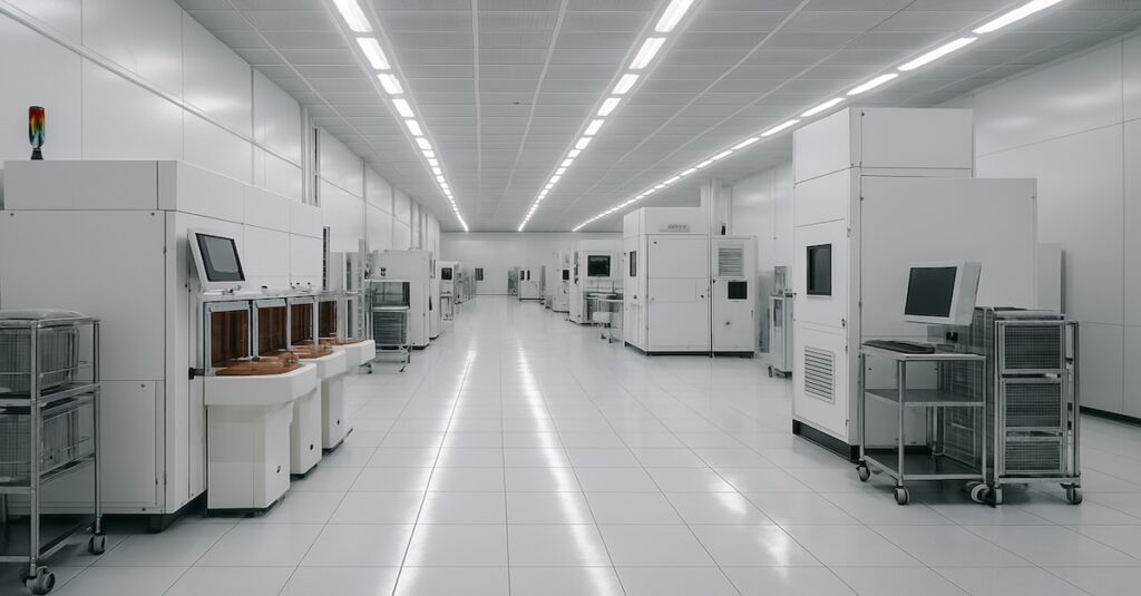
More than 50% of the semiconductor FAB (fabrication) cost is due to equipment and tools. Any given FAB has hundred different types of these, and without the required tools and equipment, the FAB cannot work efficiently. One piece of equipment that drives the semiconductor fabrication process forward is lithography.
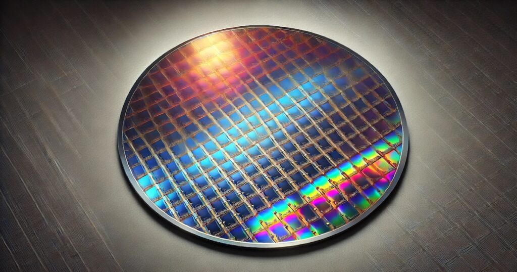
There are several aspects of semiconductor fabrication that has driven by lithography equipment. Yield and defect are two such examples from the technical point of view. It is the primary reason why semiconductor fabrication focuses a lot on which type of lithography technology to deploy. Eventually, products with low yields and high defect rates will not be market-qualified.
Yield: Lithography equipment plays a vital part in achieving the required target process yield.
Defect: Defect free masking is an important part of semiconductor fabrication made possible by lithography.
Yield and defect are also dependent on the complexity of the semiconductor product. However, lithography equipment is supposed to handle the complex process. With semiconductor manufacturers focusing on next-gen advanced technology nodes, the importance of error-free lithography equipment will increase further.
Semiconductor process technology is dependent on lithography and plays a crucial part in deciding how the FAB throughput will be. It is why semiconductor manufacturers worldwide are focused on acquiring the latest lithography equipment to upgrade existing FABs or build a new ones.

From a technical point of view, lithography equipment plays a vital role, and apart from yield and defect, there are more process-related criteria that lithography fulfills. However, from the business side too, the lithography equipment plays an important part.
Two ways in which lithography equipment helps from a business point of view are capacity and break-even point. When it comes to building or upgrading FABs, lithography decisions are crucial. The reason being the solutions that the semiconductor FAB wants to make should be proven with different process steps, including the one executed by the lithography. In many cases, lithography often becomes the bottleneck due to the complex process.
Capacity: FAB expansion and upgrade are directly related to the lithography equipment performance.
Break-Even: Lithography also plays a critical role in achieving the FAB Break-Even Point.
Semiconductor FAB capacity is directly associated with lithography due to the process node. The majority of the semiconductor FABs are opting for a new process node, and the decision on which type of xUV technology to use becomes an important parameter. Lithography also allows FABs to achieve faster break-even by continuously processing large numbers of defect-free and good-yielding wafers.
Semiconductor capacity building is speeding up, and with technical/business impacts, lithography will play a big part. There are several concerns about lithography equipment shortage, and the path to successfully operating the new FAB will not be easy. Semiconductor manufacturers will have to focus on mitigating the lithography equipment shortage so that the investment done has a long-lasting impact.


