Image Generated Using DALL-E
Precision And Semiconductors
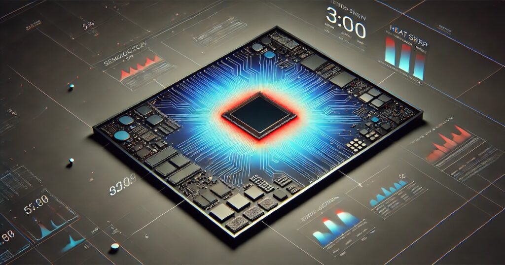
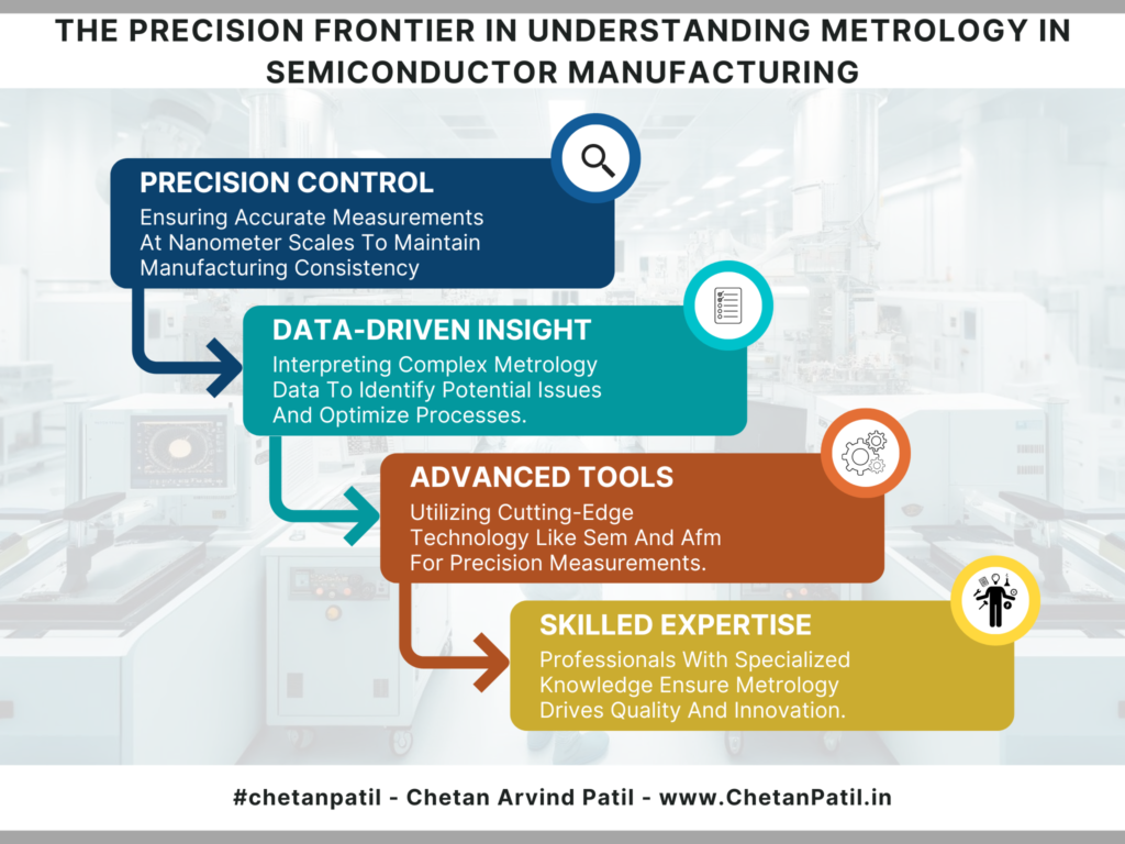
Precision is not just a technical term in semiconductor manufacturing. It is the foundation on which everything is built. As the FET devices get smaller, faster, and more advanced, the margin for error becomes razor-thin. That is where metrology comes in. It is the science of measuring, but it is much more than that in this industry.
What Is Metrology
Metrology is the science of measurement, and in semiconductor manufacturing, it ensures every tiny component on a chip is produced with extreme precision. As chips become more complex and feature sizes shrink to the nanometer scale, even the slightest error can impact the performance and reliability of devices.
Semiconductor metrology involves using advanced tools and techniques to measure everything from the thickness of materials to the alignment of circuits, ensuring that each step in the manufacturing process meets exacting standards. Without metrology, the high-performance technology we rely on, from smartphones to medical devices, would not be possible.
Application Of Metrology In Semiconductor
Metrology is applied at nearly every stage of semiconductor manufacturing to ensure precision and reliability. Here are some key areas where metrology plays a crucial role:
| Stage | Metrology Application |
|---|---|
| Wafer Production | Measures wafer thickness, flatness, and surface quality to ensure uniformity. |
| Lithography | Verifies the accuracy of patterns etched onto the wafer, measuring line widths and alignment. |
| Etching and Deposition | Monitors depth, uniformity, and precision of materials etched or deposited on the wafer. |
| Doping and Implantation | Ensures the correct concentration and placement of dopants to alter the wafer’s electrical properties. |
| Packaging and Assembly | Verifies dimensions of interconnects, bumps, and solder joints to ensure reliable connections. |
| Quality Control | Detects and identifies defects, from contamination to structural flaws, at every stage. |
| Final Testing | Measures electrical characteristics, thermal properties, and functionality of the finished product. |
Maintaining the necessary precision at these critical stages of semiconductor production without metrology would not be impossible, leading to lower yields and potentially defective chips.
Semiconductor Equipment To Enable Metrology
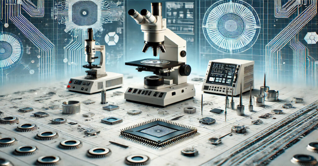
Metrology in semiconductor manufacturing highly depends on using advanced equipment to achieve the precision required at the nanometer scale. These tools ensure that each step of the process, from wafer production to final testing, meets the stringent demands of modern technology, presenting a constant challenge.
Without the right metrology equipment, measuring, monitoring, and controlling the intricate features that makeup today’s semiconductor devices would be impossible. The following table outlines vital metrology equipment and their critical applications in semiconductor manufacturing.
| Equipment | Application |
|---|---|
| Scanning Electron Microscope (SEM) | High-resolution imaging to inspect surface features and dimensions at the nanoscale. |
| Atomic Force Microscope (AFM) | Measures surface topography, roughness, and mechanical properties at the atomic level. |
| Optical Microscope | Inspects larger features and performs quick quality checks for alignment and defects. |
| X-ray Metrology Tools | Analyzes thin film thickness, composition, and structure using X-rays. |
| Ellipsometer | Measures film thickness and refractive index of deposited layers. |
| Critical Dimension Scanning Electron Microscope (CD-SEM) | Measures precise feature dimensions, such as line widths, on wafers. |
| Fourier Transform Infrared Spectroscopy (FTIR) | Identifies chemical compositions of materials used in wafer processing. |
| Profilometer | Measures surface profile and step height, often used after etching and deposition. |
| Scatterometry | Non-imaging technique to measure periodic features and critical dimensions via light diffraction. |
| Overlay Metrology Tools | Ensures proper alignment of multiple layers during chip fabrication. |
| Electrical Test Equipment | Measures electrical properties such as resistance, capacitance, and transistor performance. |
Metrology equipment is the backbone of quality control and precision in semiconductor manufacturing. Each piece of equipment serves a specific purpose, whether inspecting surface features at the atomic level or ensuring proper alignment between layers.
As semiconductor devices continue to shrink and grow in complexity, the role of metrology tools becomes even more vital in maintaining production quality, yield, and performance. It is thus crucial to invest in the right metrology equipment to keep up with current technology and drive future innovations in the semiconductor industry.
Data-Dependent Metrology
Metrology tools generate vast amounts of data, from wafer thickness measurements to defect identification at the atomic scale. This data is critical in ensuring that each semiconductor device component is within its strict design tolerances. In an industry where margins of error are measured in nanometers, capturing, interpreting, and acting on metrology data is essential to quality control and innovation. As an example:
SEM and AFM data provide insight into surface roughness and dimensions, which are crucial for ensuring the chip performs as designed.
Electrical Test Equipment is a critical player in this process, producing data on transistor performance that aids in forecasting the overall reliability and efficiency of the semiconductor.
Overlay Metrology Tools generate alignment data between layers of semiconductors, ensuring multi-layer chips are fabricated without defect.
Furthermore, this demands a specialized skill set, where engineers and technicians must be proficient in operating metrology equipment and understanding and analyzing the complex data it produces.
Talent And Skills Needed For Metrology
| Role | Description | Key Skills Required |
|---|---|---|
| Metrology Engineer | Designs and manages metrology processes, ensuring accurate measurements and improving tools/techniques. | Proficiency in metrology tools (SEM, AFM, profilometers), data analysis, troubleshooting, and semiconductor process knowledge. |
| Process Control Engineer | Monitors manufacturing processes using metrology data, ensuring stability and preventing defects. | Strong analytical skills, statistical process control (SPC), process optimization, and real-time problem-solving. |
| Data Scientist | Analyzes and interprets large datasets from metrology equipment to drive predictive analytics and process improvements. | Data analysis, machine learning (ML), programming skills (Python, R), and statistical modeling. |
| Calibration Technician | Calibrates and maintains metrology equipment to ensure precise measurements and tool reliability. | Understanding of calibration techniques, attention to detail, tool maintenance, and equipment troubleshooting. |
| Quality Assurance (QA) Engineer | Ensures all products meet quality standards by interpreting metrology data and assessing compliance. | Proficiency in quality management systems (QMS), defect detection, metrology data interpretation, and compliance auditing. |
| RnD Metrology Scientist | Develops new measurement methods and tools to support advanced semiconductor technologies. | Research skills, innovation in metrology techniques, deep knowledge of semiconductor materials, and data interpretation. |
The role of metrology in semiconductor manufacturing goes far beyond just taking measurements. It blends cutting-edge equipment, complex data interpretation, and skilled professionals, ensuring each chip performs reliably.
As semiconductor technology continues to evolve at a rapid pace (leading to much smaller devices), so will the demands placed on metrology. The professionals who bring this data to life, analyze it, and apply their insights will remain at the forefront of the semiconductor revolution, maintaining quality and driving innovation in one of the world’s most precise industries.