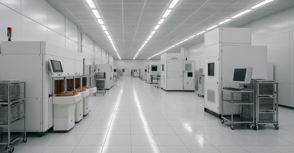
Photo by Maxence Pira on Unsplash
India is betting on end-to-end semiconductor manufacturing, which is the right step to meet the growing demand for the country’s semiconductor requirements. If executed as planned, the import of silicon chips will drastically decrease and will remove the dependency on the other countries.
The technology node is crucial to getting the semiconductor manufacturing strategy correct. It is at the core of any silicon chip that ever gets produced, and for a country like India, where the majority of the semiconductor manufacturing (mainly the FAB/fabrication part) is confined to public units and caters to the country’s space, defense, and other critical national infrastructure needs. Leveraging these foundations and extending the technology node capabilities to develop more India-centric process technologies is more beneficial.
The Technology Node (Also Process Node, Process Technology, Or Simply Node) Refers To A Specific Semiconductor Manufacturing Process And Its Design Rules.
Thus, considering the capabilities of India’s public semiconductor FAB, it is more suitable to aim for 140nm and above. The reason ranges from cost, yield, process control, and market demand. 140nm is also perfect due to the 180nm capabilities of the Semi-Conductor Laboratory, which can extend to not only develop CMOS devices to fabricate 140nm but can potentially ensure that these facilities also get upgraded – a win-win situation for all.
If the SCL cannot develop 140nm in-house, there is also a potential to tie up with established Pure-Play vendors. Similar to Maruti-Suzuki JV. Regarding market potential, 140nm CMOS, including BiCMOS semiconductor technology, is still in high demand, mainly in the industrial, automotive, mobile, and other computing sectors.

The semiconductor equipment and setup cost for 140nm and above CMOS/BiCOMS semiconductor FAB is relatively lower than the advanced nodes. Yield is better, and the application area is far greater. Focusing on anything lower, mainly the advanced nodes like 7nm, etc., will be a step in the wrong direction unless a private player is willing to set up FAB by utilizing the incentives and spending endless resources.
Benefits of 140nm and above CMOS/BiCMOS:
Proven: 140nm and above is an established and widely used technology node that can speed up India’s semiconductor fabrication and manufacturing entry.
Cost: 140nm and above is more cost-friendly, and the equipment is easy to procure, including utilizing the used equipment market.
Yield: The established knowledge around 140nm and above CMOS can ensure the bring-up time of new FAB is fast.
ROI: The break-even and ROI for 140nm and above technology nodes will be much faster than any other process node as it fits the edge of market requirements.
While having an advanced node FAB in India can be a game-changer, but only if a private player does it. If the focus is to get Indian companies to set up FAB in India (like Vedanta, etc.), creating a tech JV with SCL and other players to develop process flow for 140nm and above indigenously could be a more significant breakthrough.


